Demonstrating optical and spin coherence properties of epitaxial Er :CeO2 /Si at 4 K Purcell enhancement of Er: TiO2/Si devices via atomic layer deposition
Science: Scientists at Argonne National Laboratory and the University of Chicago demonstrate that a new method for growing erbium-doped thin films allows them to be easily integrated with silicon photonics.
Impact: These works benchmarked the potential of new on-chip and silicon-compatible qubit systems and nanophotonic devices for quantum and the first demonstration of the use of foundry scalable atomic layer deposition methods.

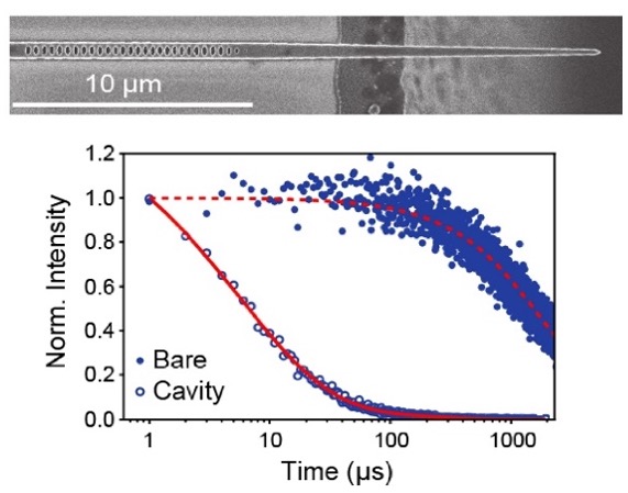
SEM image of the nanophotonic device and comparison of the ensemble lifetime of Er ions uncoupled (Bare) and coupled (Cavity), showing a Purcell enhancement of 300.
Summary: A collaboration between Argonne and the University of Chicago is investigating scalable oxides on silicon for use in quantum memories and, ultimately, repeaters for quantum communications. In recent work the investigators experimentally evaluated Er:CeO2 as such a platform, owing to the combination of the predicted long electron spin coherence time, a near lattice-match to Si, and a telecom wavelength transition. The collaboration was able to systematically evaluate the dependence of optical properties including electron paramagnetic resonance (EPR) linewidth and excited state lifetimes on doping density, as well as the spin coherence properties and limiting factors. In complementary work the groups evaluated Er:TiO2 using a foundry-scalable atomic layer deposition (ALD) process with part-per-million doping control demonstrated for the first time, versus previous experiments using devices grown by MBE. Structures were coupled to 1D Si photonic crystal cavities to achieve Purcell enhancement in excess of 300, which reduced Er emission time from 1718 μs to 5.7 μs
Contact: Supratik Guha, guha@uchicago.edu
Institutions: Argonne National Laboratory, University of Chicago
Focus area: Quantum materials and devices
Citation: C. Ji, M. T. Solomon, G. D. Grant, K. Tanaka, M. Hua, J. Wen, S. K. Seth, C. P. Horn, I. Masiulionis, M. K. Singh, S. E. Sullivan, F. J. Heremans, D. D. Awschalom, S. Guha, A. M. Dibos. “Nanocavity-mediated purcell enhancement of Er in TiO2 thin films grown via atomic layer deposition.” ACS Nano 2024, 18, 14, 9929–9941. doi:10.1021/acsnano.3c09878
Funding acknowledgment: The authors acknowledge the Q-NEXT Quantum Center, a U.S. Department of Energy, Office of Science, National Quantum Information Science Research Center, under Award Number DE-FOA-0002253 for support (C.J., G.D.G., C.P.H., I.M., S.K.S, D.D.A., S.G., and A.M.D.). AFM characterization, oxygen annealing, electron microscopy, and cavity device fabrication were performed at the Center for Nanoscale Materials, a U.S. Department of Energy Office of Science User Facility, supported by the U.S. DOE, Office of Basic Energy Sciences, under Contract No. DE-AC02-06CH11357. Additional support (M.H. and J.W.) for TEM characterization is supported by Quantum Information Science research funding from the U.S. DOE, Office of Science User Facility. Additional materials characterization support (M.T.S., S.E.S., and F.J.H.) was provided by the U.S. Department of Energy, Office of Science; Basic Energy Sciences, Materials Sciences, and Engineering Division. Additional support (M.K.S.) for growth capabilities was provided by the Center for Novel Pathways to Quantum Coherence in Materials, an Energy Frontier Research Center funded by the U.S. Department of Energy, Office of Science, Basic Energy Sciences under Award No. DE-AC02-05CH11231.