Demonstrating optical and spin coherence properties of epitaxial Er :CeO2 /Si at 4 K
Purcell enhancement of Er: TiO2/Si devices via atomic layer deposition
The Science:
Scientists at Argonne National Laboratory and the University of Chicago work toward a foundry-scalable and CMOS-compatible thin film growth method for erbium-doped quantum memories.
The Impact:
The group’s scalable quantum memory devices, which operate at telecom wavelength, could enable myriad quantum technologies – including quantum repeaters for worldwide quantum networks.
Summary:
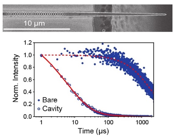
A collaboration between Argonne and the University of Chicago demonstrated an easy and uniform atomic-layer deposition (ALD) of erbium-doped titanium dioxide films. A pulse sequence enables an erbium doping range from under the parts-per-millions (ppm) scale to few atomic percent alloys. Low doping levels are rare for ALD processes. The amorphous as-grown films transition to an anatase phase after a 400-degree-Celsius oxygen anneal, but critically, the surface remains very smooth after the annealing process. The erbium telecom-wavelength emission improves greatly after crystallization. The thin films can be patterned into nanoscale optical cavities with high quality factors, demonstrating a Purcell enhancement of erbium emission up to 300.
Contact:
Supratik Guha, guha@uchicago.edu
Institutions:
Argonne National Laboratory, University of Chicago
Focus areas:
Quantum materials and devices
Citation:
C. Ji, M. T. Solomon, G. D. Grant, K. Tanaka, M. Hua, J. Wen, S. K. Seth, C. P. Horn, I. Masiulionis, M. K. Singh, S. E. Sullivan, F. J. Heremans, D. D. Awschalom, S. Guha, A. M. Dibos. “Nanocavity-mediated Purcell enhancement of Er in TiO2 thin films grown via atomic layer deposition.” ACS Nano 2024, 18, 14, 9929–9941.
Funding acknowledgement:
The authors acknowledge the Q-NEXT Quantum Center, a U.S. Department of Energy, Office of Science, National Quantum Information Science Research Center, under Award Number DE-FOA-0002253 for support (C.J., G.D.G., C.P.H., I.M., S.K.S, D.D.A., S.G., and A.M.D.). AFM characterization, oxygen annealing, electron microscopy, and cavity device fabrication were performed at the Center for Nanoscale Materials, a U.S. Department of Energy Office of Science User Facility, supported by the U.S. DOE, Office of Basic Energy Sciences, under Contract No. DE-AC02-06CH11357. Additional support (M.H. and J.W.) for TEM characterization is supported by Quantum Information Science research funding from the U.S. DOE, Office of Science User Facility. Additional materials characterization support (M.T.S., S.E.S., and F.J.H.) was provided by the U.S. Department of Energy, Office of Science; Basic Energy Sciences, Materials Sciences, and Engineering Division. Additional support (M.K.S.) for growth capabilities was provided by the Center for Novel Pathways to Quantum Coherence in Materials, an Energy Frontier Research Center funded by the U.S. Department of Energy, Office of Science, Basic Energy Sciences under Award No. DE-AC02-05CH11231.