Studying the formation dynamics of divacancy spin qubits in 4H-SiC using high-resolution synthesis and strain imaging.
Science: Scientists at Argonne National Laboratory, Sandia National Laboratories, the University of Chicago, and the University of Glasgow demonstrate a method for implanting qubits in silicon carbide with extreme precision and analyze how silicon carbide responds at the atomic scale to the qubits’ implantation.
Impact: By combining capabilities from three DOE-SC User Facilities (APS, CNM, CINT), researchers have paved the way for a quantitative understanding of defect synthesis in SiC and other materials.
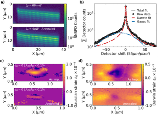
a) PL of VV0 obtained via Si++ implantation of 4H-SiC vs fluence. b) Example of two component quantitative strain fitting model for 10000 ions/spot. c) 2D tensile strain ε profile of a nanoimplanted spot, extracted from the Gaussian component. d) strain response of the host 4H-SiC crystal extracted from the Darwin component. Both c) and d) are for 10000 ions/spot.
Summary: The deterministic creation of divacancies in silicon carbide (SiC) were performed via nanoimplantation (~60 nm) using a focused ion beam at the Center for Integrated Nanotechnologies (CINT). Confocal microscopy revealed that thermal processing is key in achieving bright emitters. Researchers created a quantitative X-ray diffraction map of the pre- and postannealed implantation zones performed with 10-6 strain sensitivity using the hard X-ray nanoprobe at the Advanced Photon Source (APS) and Center for Nanoscale Materials (CNM). They observed a qualitative model with a tensile core and compressive implantation zone and with thermally induced isotropic diffusion of strain. Follow-up studies focused on reducing implanted versus interrogated volumes for improved signal/noise analysis and single defect sensitivity.
Contact: Nazar Delegan, ndelegan@anl.gov
Focus area: Quantum materials characterization
Institutions: Argonne National Laboratory, Sandia National Laboratories, University of Chicago, University of Glasgow
Citation: N. Delegan, S. J. Whiteley, T. Zhou, S. L. Bayliss, M. Titze, E. Bielejec, M. V. Holt, D. D. Awschalom, F. J. Heremans. “Deterministic nanoscale quantum spin-defect implantation and diffraction strain imaging.” Nanotechnology 34, 38 5001. (2023)
Funding acknowledgement: This material and effort is based upon work primarily supported by the U.S. Department of Energy Office of Science National Quantum Information Science Research Centers as part of the Q-NEXT center (ND, MH, DDA, and FJH). Additional support for preliminary measurements was funded by the U.S. Department of Energy, Office of Basic Energy Sciences, Materials Science and Engineering Division (SJW). This work was performed, in part, at the Center for Integrated Nanotechnologies, an Office of Science User Facility operated for the U.S. Department of Energy (DOE) Office of Science. Sandia National Laboratories is a multi-mission laboratory managed and operated by National Technology & Engineering Solutions of Sandia, LLC, a wholly owned subsidiary of Honeywell International, Inc., for the U.S. DOE’s National Nuclear Security Administration under contract DE-NA-0003525. The views expressed in the article do not necessarily represent the views of the U.S. DOE or the United States Government. SLB acknowledges support from UK Research and Innovation [Grant: MR/W006928/1]. Work performed at the Center for Nanoscale Materials and Advanced Photon Source, both U.S. Department of Energy Office of Science User Facilities, was supported by the US DOE, Office of Basic Energy Sciences, under Contract No. DE-AC02-06CH11357.